|
|
|
|
|
| Electronic component procurement |
|
|
| IC integrated circuit programming |
|
|
|
|
|
|
|
 |
| PCB soldering service |
|
|
Daily Production Points: 5 million
PCBA Production Size: Maximum 490 x 810MM
Board Thickness Range: 0.3-6.5MM
Order Quantity: 1-100,000pcs
Electronic Components: ① Passive components, minimum package 01005; ② Minimum lead pitch can be as low as 0.25mm
Soldering Types: Through-hole components (DIP devices) / Surface mount components (SMT devices) / Hybrid surface mount and through-hole components / Double-sided component soldering (including surface mount and through-hole)
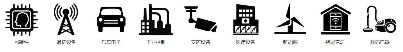
Application Areas: Artificial intelligence hardware, communication equipment, automotive electronics, industrial control, security, medical, IoT, etc.
|
|
|
| SMT patch |
|
Sample processing |
|
Small batch PCB soldering service |
|
DIP plugin |
|
BGA soldering |
|
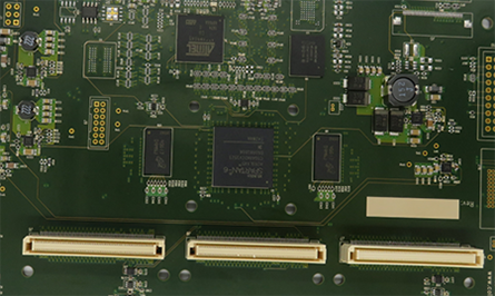
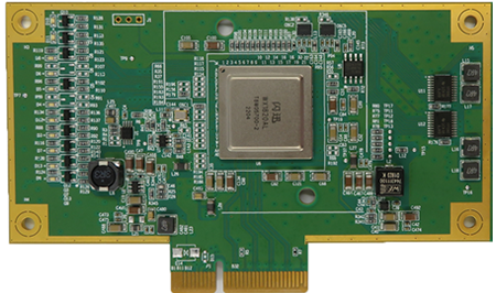
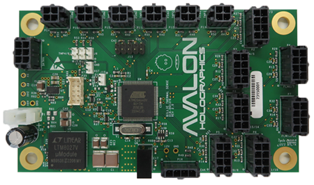
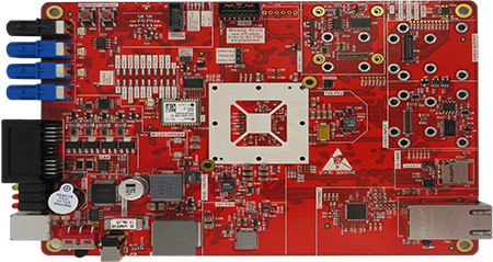
PCBA Sample Display |
|
|
| SMT assembly process |
 |
|
|
Standard Delivery Time
Standard Sampling (within 50pcs): 3 days for complete materials
Small Batch (50-500pcs): 3-5 days
Batch (≥500pcs): 5-7 days
|
|
PCBA Circuit Board Dimensions
Small Board Size: 50mm x 50mm
(Smaller boards require panelization)
Large Board Size: 810 * 490mm
|
|
Daily Production Capacity
PCBA SMT: 324,000-810,000 points/day
|
|
Ball Grid Component (BGA) Spacing
Not less than 0.35mm
Conformal coating
|
|
|
Types of PCB Boards Available
Rigid PCB (FR-4, Metal Substrate)
Flexible PCB (FPC)
Rigid-Flex PCB
Aluminum Substrate
|
|
Component Mounting Accuracy
Minimum component accuracy ±0.04mm
IC surface mount accuracy ±25μm
|
|
Component Services
Full-service component delivery
Partial component delivery
OEM/ODM component delivery
|
|
Component Size
CHIP 01005 (Metric 0.3*0.15mm)~45mm
High-precision ICs such as BGA: Supports X-ray inspection of BGA components with a minimum pitch of 0.25mm
|
| SMT assembly process |
|
|
|
01-IQC Incoming Material Inspection
Inspection Purpose: To prevent process defects caused by defective materials on the production line, thus delaying delivery.
|
|
|
|
02-SPI solder paste testing
Inspection Objective: To detect early signs of work flowing from one process to the next.
Inspection Standard: 3D inspection + data statistical analysis
|
|
|
|
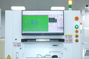
03-Online 3D AOI Inspection
Inspection purpose: To check whether there are any errors, omissions, or defects in the manufactured products, and whether any substandard materials have flowed into the next process.
|
|
|
|
04-SMT First Article Inspection
Inspection Purpose: To ensure that the components affixed to the production model completely match the customer's assembly drawings and bill of materials, preventing defective components from flowing into the next process.
Inspection Standards: Refer to BOM and Gerber data.
|
|
|
|
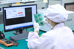
05-Appearance inspection
Inspection Purpose: To conduct a full inspection of the manufactured products to ensure they conform to the work instructions.
Inspection Standards: Process instructions for each product and work instructions for each position.
|
|
|
|
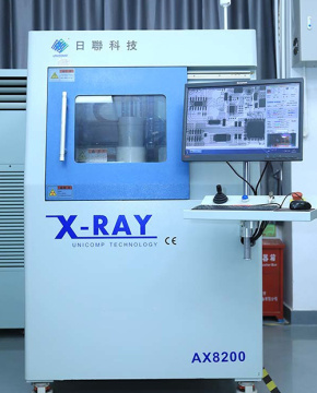
06-X-ray-Welding inspection
Inspection Purpose: To inspect solder joints of components that are not visible to the naked eye to prevent cold solder joints and short circuits from being discharged to the next process.
Inspection Equipment: Nichiren AX8200
|
|
|
|
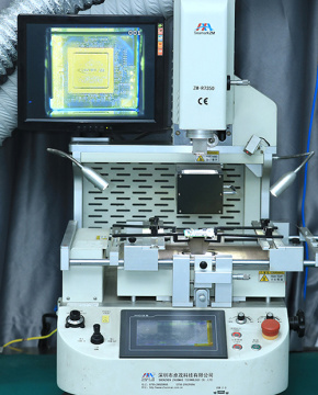
07-BGA device repair
X-ray inspection of BGA soldering defects involves disassembly and soldering under controlled temperature conditions to mitigate the impact on components and ensure the quality of solder repair.
|
|
|
|
08-QA testing
Standardize finished product inspection before shipment to prevent defective products from being shipped.
Use anti-static packaging and secure warehousing before shipping via SF Express.
|
|
| SMT Workshop Error Prevention System |
|
|
|
1. Glue Application Board: Tests the correct placement of SMT components, significantly reducing SMT trial production time and component waste, effectively ensuring SMT quality;
2. Intelligent First Article Inspection Instrument: Detects incorrect components, missing components, polarity, orientation, silkscreen printing, etc., mainly used for first article inspection; compared to manual inspection, it is more accurate and faster by 50%+;
3. SPI-Fully Automatic 3D Solder Paste Thickness Gauge: Detects various solder paste printing quality problems such as missing prints, insufficient solder, excessive solder, solder bridging, misalignment, poor shape, and board surface contamination;
4. 3D Online AOI: Detects various problems after placement: short circuits, missing components, polarity, misalignment, and incorrect components;
5. X-ray: Performs open circuit and short circuit detection on BGA, QFN, and other components.
|
|
 |
| SMT assembly equipment |
|
|
 |
|
 |
|
 |
|
 |
|
 |
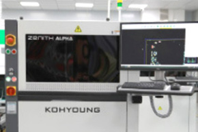
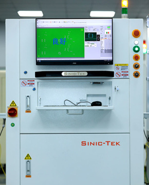
| X-RAY |
|
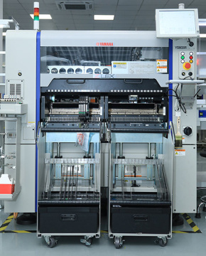
SMT placement machine |
|
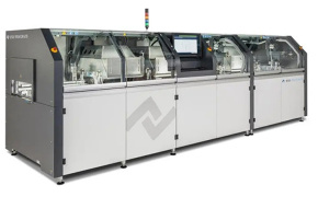
ERSA Selective Wave Soldering |
|
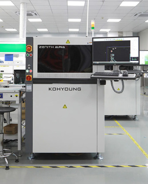
3D Online AOI |
|
RGA Repair Station |
 |
|
 |
|
 |
| Wave soldering |
|
Loading machine + printing machine |
|
Reflow soldering |
 |
|
 |
|
 |
|
 |
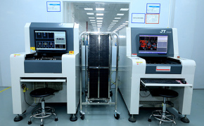
| Online SPI |
|
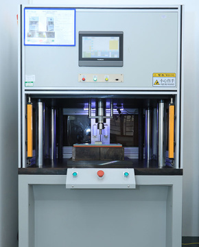
Crimping machine |
|
Offline AOI |
|
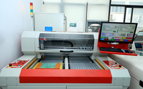
PCBA depaneling machine |
| SMT assembly plant qualifications |
|
|
|
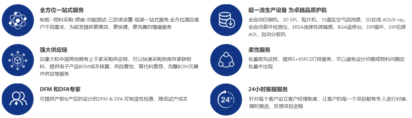
Juyuan Union Technology (Shenzhen) Co., Ltd. is certified to ISO9001 Quality Management System and ISO13485 Medical Device Quality Management System. It boasts a strong engineering quality management team and a professional electronic component procurement team. Products comply with IPC-A-600 & IPC-A-610 standards, ensuring that the quality and production technology of all company products meet international standards and customer requirements. The company provides value-added services to satisfy customers, such as Design for Manufacturability (DFM/DFA), helping customers smoothly transition from design to mass production as a one-stop PCB service provider.
Founded in 2010, Juyuan Union has its production and operation base in Zhaoqing, China, with sales centers in Shenzhen, Guangzhou, and Zhejiang, providing high-quality services to over 3,000 customers worldwide. Juyuan Union's future goal is to establish the world's largest rapid manufacturing platform in the field of PCB prototyping and multi-variety, small-batch production. With its market positioning of "multi-variety, small-batch, short-lead-time," stable delivery times, and excellent quality assurance, it has built the HuaSin brand in the global PCB market. The number of product varieties delivered reaches 4,000 per month. For four-layer products, the fastest delivery time is 24 hours; for six-layer products, the fastest delivery time is 48 hours; and for eight-layer products and above, the fastest delivery time is 72 hours.
|
 |
|
 |
| SMT assembly processing application areas |
|
|
| Why Choose Juyuan Union for SMT Assembly? |
|
|
|
|
|
|
Our company provides rapid prototyping and sample manufacturing services. There are no restrictions on order quantity, ranging from 1 piece to bulk production. Through prototyping services, we can help customers identify design or material issues in advance, avoiding losses during mass production and assisting customers in a smooth transition from prototyping to mass production. We also provide customers with DFM pre-production inspection and DFA post-production manufacturability inspection services to help them identify problems in advance, save time and costs, summarize hidden design issues discovered during the manufacturing process, and reduce trial production costs.
|
| Sample line processing capabilities |
| Line Number |
PCB Size for Small and Medium Batch Production |
Material Sizes Available for Small and Medium Batch Production |
PCB Thickness/Material Height |
Minimum Ball Pitch for BGA/IC Mounting |
| LINE1 (GKG Printer + YSM20 + YSM20 Tray) |
50*50-810*490mm |
CHIP 0201 (Metric 0.5*0.25mm) - 32mm |
0.3-6MM/15MM |
0.4MM |
LINE2 (GKG printing press + YSM20 + YSM20 pallet)
50*50-810*490mm
CHIP 0201 (Metric 0.5*0.25mm) - 32mm
0.3-6MM/15MM
0.4MM
LINE3 (GKG printing press + Desen printing press + YS12 + YS12 modification)
50*50-510*415mm
CHIP 03015 (Metric 0.3*0.15mm) - 32mm
0.3-6MM/15MM | 0.35MM |
| LINE4 (Plate Feeder + Desen Printing Machine + YS12 + YSM20R) |
50*50-810*350mm |
CHIP 03015 (Metric 0.3*0.15mm) - 45mm |
0.3-6MM/15MM |
0.35MM |
|
|
|
|
|
Small-batch PCB soldering refers to the assembly and soldering of circuit boards ranging from 25 to 5000 pieces, including DFM and DFT. Juyuan Union provides a complete small-batch soldering service, including bare PCB boards, material procurement, and final soldering assembly.
DFM is essential for small-batch soldering. We will review your Gerber files, BOM, assembly files, and circuit diagrams to prevent any engineering problems. As an electronics outsourcing service provider, we will reduce costs by optimizing PCB panelization to facilitate soldering operations. We also recommend using solder mask openings to achieve high throughput and prevent short-circuit bridges. Before procuring materials, we will conduct a comprehensive matching check between your component list and PCB files. This effectively avoids wasted costs and delayed delivery.
Similarly, even in small-batch soldering, DFT should be considered in your circuit design. Various probe test models and test limitation instructions can be provided. You will receive professional guidance on how to identify test points. We can provide comprehensive testing of your motherboard to meet your testing requirements through your troubleshooting guide, diagnostic tests, and related documentation.
We ensure your small-batch soldering is risk-free through various methods. All circuit boards in our full-service package undergo electrical testing. We can also send you pre-made boards for testing before soldering the rest. X-ray testing is used to inspect the soldering quality of BGAs and components without external leads. We can resolve any soldering issues before shipment.
We minimize the cost of small-batch soldering as much as possible. There are no NRE or stencil fees for repeat orders. We compare material prices among major suppliers, selecting those with high quality and low prices to reduce material costs. We have established strong partnerships with major suppliers in the US, providing competitive prices while ensuring quality. We guarantee you will receive high-quality, reasonably priced, and timely delivery services with our full PCBA package.
How to Get a Formal Quote Before Placing an Order
To receive a quote for our small-batch PCB soldering service, please send your BOM and Gerber files to info@jyzltech.com.
|
 |
|
|
|
|
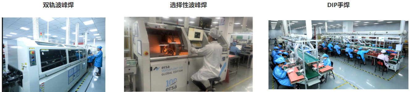
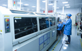
Juyuan Union Technology (Shenzhen) Co., Ltd. is a professional processing factory with many years of experience in SMT (Surface Mount Technology) assembly, component insertion, post-soldering, and assembly. Currently, it has 5 DIP production lines, offering three soldering processes and equipment: chain-type wave soldering lines, fully automated selective wave soldering lines, and manual post-soldering assembly lines, with a daily capacity exceeding 10,000 pieces.
The DIP production lines are equipped with 3D AOI (On-line Inspection) equipment to effectively prevent defects such as insufficient solder, excessive solder, solder bridging, missing leads/components, open solder joints, and cold solder joints/solder holes. The fully automated ERSA (Selective Wave Soldering) system boasts extremely high speed and precision, completing complex soldering tasks in a very short time. Due to the short localized heating time of the substrate during soldering, the heat-affected zone of the substrate is small, and the precision and hardness of the material are maintained after soldering, resulting in excellent solder joint clarity and high consistency. The ALPHA solder bars used in the DIP manual soldering lines also offer advantages such as high solder joint gloss and a full, aesthetically pleasing solder joint shape. Each production line is equipped with professionally designed workbenches, railcars, carriers, moving tracks, and fully automated PCB sorting and washing machines, along with related operating tools, effectively improving the efficiency of DIP assembly. Simultaneously, the company continuously improves its employee management mechanism for DIP assembly, assigning dedicated personnel to specific positions, implementing fixed-piece pay, and strictly controlling quality to ensure that DIP assembly meets customer quality management requirements. The company also develops standardized operating guidelines for different processes to guide the operational quality of DIP assembly line employees, strengthen the optimization and improvement of production processes, and increase the product qualification rate to a target of 99.8%, minimizing customer costs and creating value for customers.
|
JT-SMART-450-M wave soldering machine |
|
ERSA soldering option VERSAFLOW 335 |
Preheating Zone |
3 Temperature Zones |
Preheating Zone Type |
Bottom Medium Wave Infrared
Top Hot Air Convection |
Preheating Zone Temperature Control Range |
Ambient Temperature - 230°C |
Preheating Zone Temperature Control Range |
Ambient Temperature - 200°C |
Tin Furnace Temperature Control Range |
Ambient Temperature - 300°C |
Soldering Module Temperature Control Range |
Ambient Temperature - 300°C |
| height="40"> Browser PCBA Board Minimum Dimensions |
Length Unlimited, Width 50-450mm |
Soldering Positioning Accuracy |
± 0.25 mm |
Transport Speed |
500-1800mm/min |
Transport Speed |
200-10000mm/min |
Cooling Method |
Air Cooling |
PCB Width |
60-508mm |
| height="40"> PCB component height |
Top 120mm/Bottom 25mm |
PCB length |
120-508mm |
|
|
PCB edge |
5mm |
|
|
PCB component height |
Top 120mm/Bottom 30mm |
|
|
Jig/PCB weight |
8KG |
|
|
|
|
BGA Soldering and X-ray Inspection Services
Juyuan Union has been providing BGA soldering, BGA rework, and BGA ball-mounting services in the electronics manufacturing services industry for over a decade. Through our BGA rework stations, proper BGA soldering procedures, and X-ray testing, we can provide you with high-quality and high-performance BGA circuit boards.
BGA Soldering Capabilities
We have extensive experience in soldering various types of BGAs, from small (2mm x 3mm) to large (45mm), ceramic to plastic.
BGA Soldering Process
SMT BGA components are highly humidity-sensitive components, so they must be stored under constant temperature and dry conditions to avoid being affected before mounting and soldering. The ideal storage environment for BGAs is a temperature of 20℃~25℃ and a humidity of less than 10%RH (nitrogen protection is even better). If a BGA has been opened for more than the specified time (24 hours), it needs to be re-baked to prevent moisture from affecting soldering quality or altering electrical properties. This helps eliminate internal moisture, improves heat resistance, and reduces the impact of thermal shock during reflow soldering. Baking conditions are: temperature 125℃, relative humidity ≤60%RH, time 4~10 hours. After baking, remove and allow to cool naturally for half an hour before proceeding with the work.
SMT BGA Soldering Process:
Flow: Automatic board feeder => Automatic solder paste printer => SPI solder paste inspection => High-speed pick and place machine => General-purpose pick and place machine => Reflow soldering => AOI inspection => X-ray inspection (BGA)
BGA Stencil Selection: BGA components have small lead pitch, therefore the stencil thickness is thinner; generally, the stencil thickness is 0.1~0.15mm. The stencil opening depends on the component, usually slightly smaller than the solder pad by 10%.
BGA Printing: A 60-degree stainless steel squeegee is used for solder paste printing. The printing pressure is controlled within the range of 3~4kg, and the printing speed is controlled between 10mm/s and 25mm/s. The smaller the BGA lead pitch, the slower the printing speed. The stencil removal speed after printing is generally set to 1mm/s. The ambient temperature is controlled at around 25℃, and the humidity is around 55%RH.
SPI Solder Paste Inspection: After solder paste printing, it undergoes 100% inspection using a 3D SPI solder paste inspection machine to ensure good printing quality before BGA placement.
BGA Placement: A Yamaha YSM20 series pick-and-place machine is used to precisely place BGAs into their designated positions on the PCB board using mirror optical recognition. BGAs must not be misaligned, floating, or uneven. During production, X-ray sampling is used periodically to control BGA placement and ensure good quality.
BGA Reflow: a. Heating Zone: During this phase, the PCB is heated evenly to stimulate flux activity. The temperature rise should not be too rapid to prevent PCB deformation. The temperature rise should ideally be controlled at 3℃/second for 60-90 seconds; b. Preheating Zone: The flux begins to evaporate. The temperature is 150℃-180℃ for 60-120 seconds, with a temperature rise of 0.3-0.5℃/second to ensure the flux is fully effective; c. Reflow Zone: The temperature has exceeded the solder paste's melting point, turning it liquid, and soldering begins on the leads. At temperatures above 183℃, the time should be controlled at 60-90 seconds. Too long or too short a time will cause soldering problems. The time is particularly critical at 240-250℃ (lead-free solder paste), ideally controlled at 10-20 seconds; d. In the cooling zone, the solder paste begins to solidify, and the components are fixed to the circuit board. Cooling must be controlled at 3°C/second; too rapid a temperature drop can cause cold deformation during circuit board production, leading to BGA soldering problems, especially cold solder joints on the outer ring leads of the BGA.
X-RAY Inspection: After reflow soldering, the BGA is inspected using an X-RAY machine to ensure proper lead soldering. If any defects are found, feedback is provided to the preceding process for analysis and improvement.
BGA Rework / Ball Repositioning
1. BGA Ball Repositioning Repair Process
Clean any residual solder on the BGA pads using a soldering iron and desoldering wick. Clean any residual rosin on the components with alcohol. Then, fix the components to the ball repositioning base, apply flux, and use an appropriately sized stencil. Adjust the stencil to align with the pads. Use a brush to sweep solder balls into the stencil holes, ensuring each mesh is filled with solder balls. Remove the components and use rework equipment at an appropriate temperature for reflow until the solder balls are soldered to the pads.
2. BGA Printing Repair Process
Clean the solder paste residue on the BGA pads using a soldering iron and desoldering wick. Clean any remaining rosin on the components with alcohol. Then, fix the components to the ball bearing base, apply flux, and use an appropriately sized stencil. Adjust the stencil to align with the pads. Use a squeegee to print solder paste onto the component pads. Remove the components and rework them using rework equipment at an appropriate temperature to re-solder the solder paste.
X-ray Inspection After BGA Rework
We use a 3D X-ray machine to inspect for various problems that may occur during BGA soldering. X-ray inspection eliminates issues such as solder bridging between balls and uneven ball melting. Simultaneously, the X-ray equipment can accurately calculate the ball spacing to ensure the soldering meets IPC Level 2 standards. Our technicians can use X-ray inspection to detect issues such as PCB inner layer vias and BGA solder ball short circuits, cold solder joints, and other problems.
|
 |
|
|
|
 |
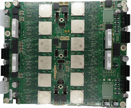
Signal Processor Motherboard
Points: 517
Component Types: 114
PCB Size: 150*200mm
Double-sided reflow + wave soldering
Minimum Package Size for RC inductors: 0402
Minimum Pin Pitch: 0.5mm
|
|
|
 |
Network Controller
Points: 306
Component Types: 54
PCB Size: 72*165
Double-sided reflow + selective wave soldering
Minimum Package Size for RC Inductors: 0402
Minimum Pin Pitch: 0.5mm
|
|
|
 |
Industrial control equipment interface board
Points: 143
Component Types: 41
PCB Size: 70*120
Double-sided reflow + selective wave soldering
Minimum Package Size for RC inductors: 0402
Minimum Pin Pitch: 0.5mm
|
|
|
 |
Security monitoring technology motherboard
Points: 711
Component Types: 192
PCB Size: 127*178mm
Double-sided reflow + wave soldering
Minimum Package Size for RC Inductors: 0402
Minimum Pin Pitch: 0.4mm
|
|
|
 |
Medical device motherboard
Number of points: 308
Component types: 77
PCB size: 304*535
Double-sided reflow + wave soldering + pressure bonding
Minimum package size for resistors, capacitors, and inductors: 0402
Minimum pin pitch: 0.5mm
|
|
|
 |
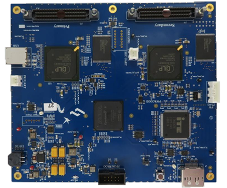
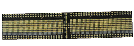
Integrated control board
Number of points: 137
Component types: 11
PCB size: 328*679
Double-sided reflow
Minimum package size for resistors, capacitors, and inductors: 805
Minimum pin pitch: 0.5mm
|
|
|
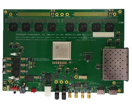 |
Fiber optic communication motherboard
Points: 1876
Component Types: 74
PCB Size: 160*233mm
Double-sided reflow + wave soldering + pressure bonding
Minimum Package Size for RC Inductors: 0402
Minimum Pin Pitch: 0.4mm
|
|
|
 |
Communication control motherboard
Points: 640
Component Types: 119
PCB Size: 140*160
Double-sided reflow + selective wave soldering
Minimum Package Size for RC Inductors: 0402
Minimum Pin Pitch: 0.4mm
|
|
|
 |
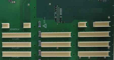
Industrial control equipment motherboard
Points: 1374
Component Types: 91
PCB Size: 183*214mm
Double-sided reflow + selective wave soldering
Minimum Package Size for RC inductors: 0402
Minimum Pin Pitch: 0.4mm
|
|
|
 |
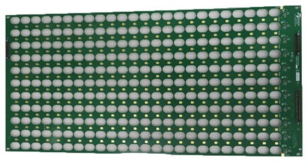
Pilot Lighting Mainboard
Points: 1039
Component Types: 36
PCB Size: 65.5*325mm
Double-sided reflow
Minimum Package Size for RC Inductors: 0402
Minimum Pin Pitch: 0.5mm
|
|
|
|
|
|
|
|
|
|
|
|
|
|