|
|
|
|
|
| Electronic component procurement |
|
|
| IC integrated circuit programming |
|
|
|
|
|
|
|
 |
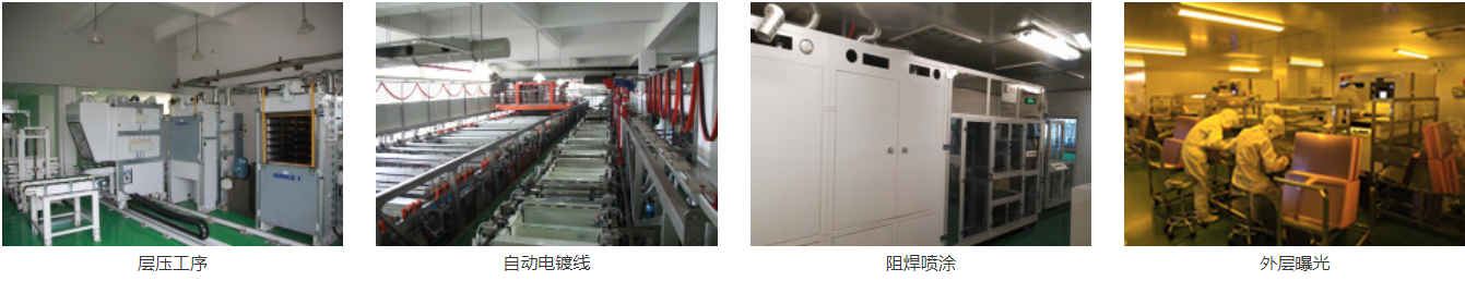
| PCB manufacturing |
|
|
Juyuan Union Technology (Shenzhen) Co., Ltd. provides printed circuit board (PCB) manufacturing services, offering PCBs with consistently high quality and reasonable prices. Whether for samples or small to medium batch production, Juyuan Union can meet your PCB manufacturing needs across various materials and technologies. We specialize in multilayer PCBs, impedance control boards, and HDI boards of varying complexity, and we offer a variety of free, high-quality solutions to ensure our customers always receive the best products.
|
|
|
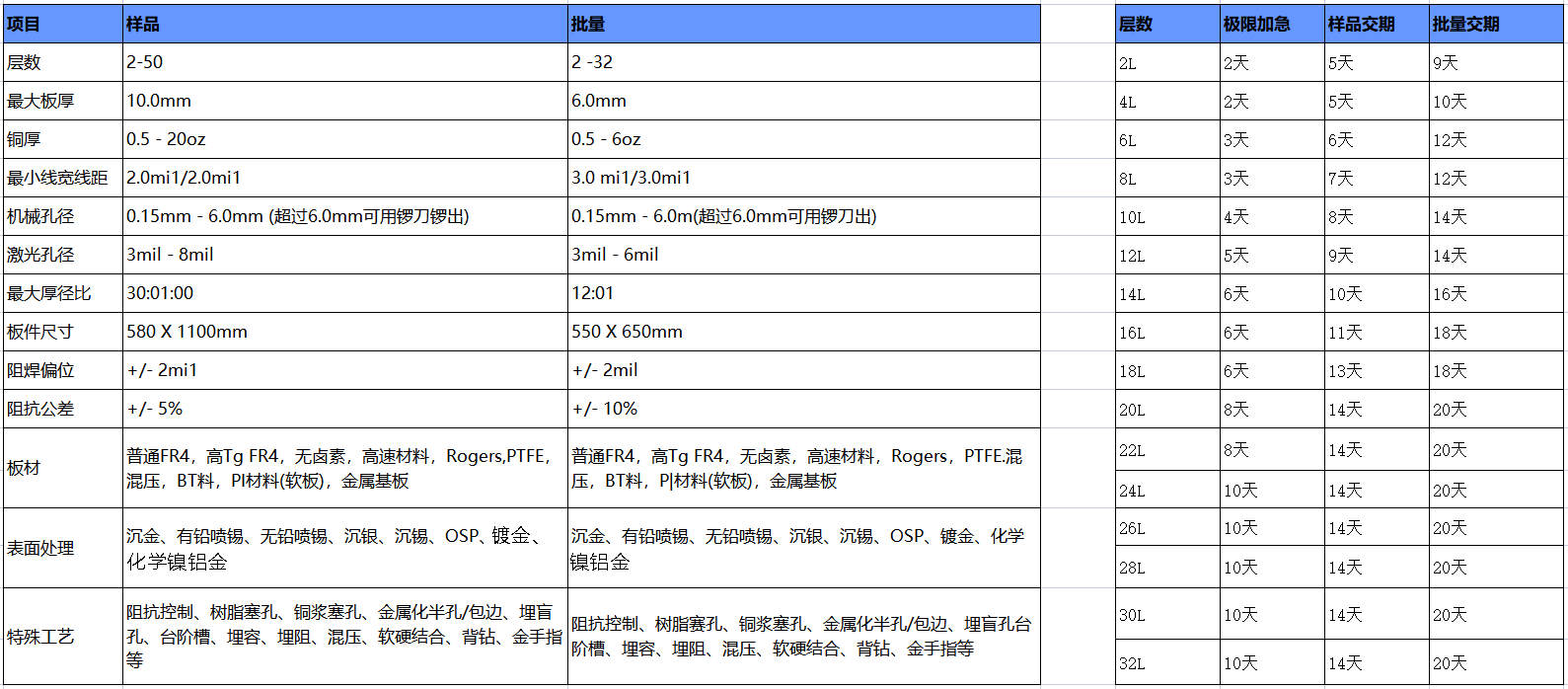
| PCB manufacturing capabilities |
|
PCB board |
|
HDI board |
|
Impedance control |
|
PCB electrical testing |
|
PCB Sample Display |
|
|
| PCB manufacturing capabilities |
 |
|
|
Juyuan Union Technology (Shenzhen) Co., Ltd. provides printed circuit board (PCB) manufacturing services, offering PCBs with consistently high quality and reasonable prices. Whether for samples or small to medium batch production, Juyuan Union can meet your PCB manufacturing needs across various materials and technologies. We specialize in multilayer PCBs, impedance control boards, and HDI boards of varying complexity, and we offer a variety of free, high-quality solutions to ensure our customers always receive the best products.
|
|
|
|
|
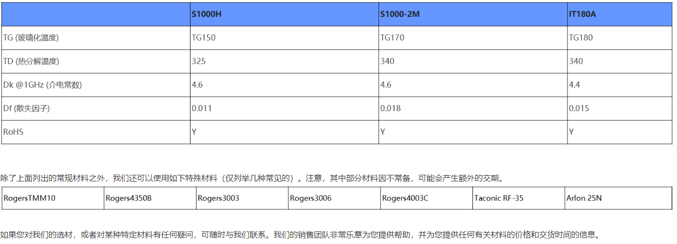
To help our clients reduce product costs and accelerate delivery times, we typically use existing board materials for PCB fabrication. However, for some of your designs that may require very specialized materials to meet functional requirements, we can also fabricate boards according to your specifications. We can also use some unconventional materials upon request, such as Rogers, Isola 370HR, FR408HR, etc., to meet your needs. We maintain ample stock of standard boards; as long as we have the boards you choose in stock, it won't affect the PCB manufacturing and soldering delivery time.
What differentiates Juyuan Union Technology (Shenzhen) Co., Ltd. from our competitors? Often, many processing plants prioritize low costs, neglecting quality and service. Juyuan Union strives to minimize costs while providing the highest quality PCB fabrication and soldering. When selecting PCB boards, we use the highest quality boards available and refuse to use low-quality boards. The table below lists our standard materials.
|
|
 |
|
|
|
|
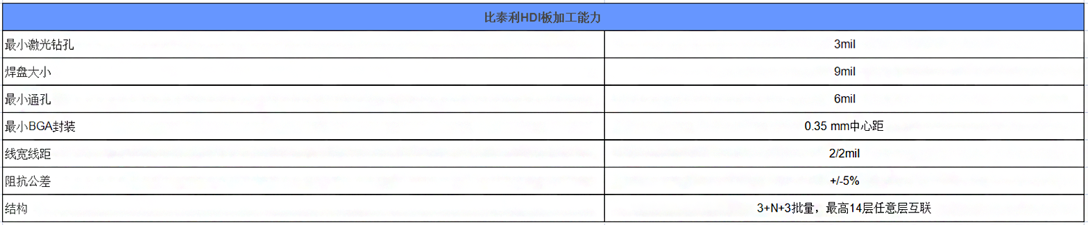
Since 2016, Juyuan Union Connectivity has officially incorporated HDI board processing and soldering into its manufacturing capabilities to enhance its overall strength. We are pleased to offer you HDI board processing and soldering services.
HDI boards have denser wiring and pads than traditional printed circuit boards. Their characteristics are reflected in finer lines, smaller spacing, smaller pads, and the use of microvias. As consumer electronics products become increasingly smaller, the market demand for lighter, thinner PCBs with lower loss under high-speed signals is growing rapidly, and the demand for HDI board processing is also steadily increasing.
Due to market demand for HDI board manufacturing, Juyuan Union has provided services to customers in many industries, including:
1. Automotive (engine control unit, GPS, dashboard electronics)
2. Computers (laptops, tablets, wearable electronics, IoT)
3. Communications (mobile phones, modules, routers, switches)
4. Digital products (cameras, audio, video)
The table below shows our HDI board processing capabilities:
|
 |
|
Juyuan Union is committed to continuously improving and perfecting our HDI board manufacturing services.
For more detailed information about the HDI technology we use, or any questions about the HDI board PCB soldering and assembly process, please feel free to contact us.
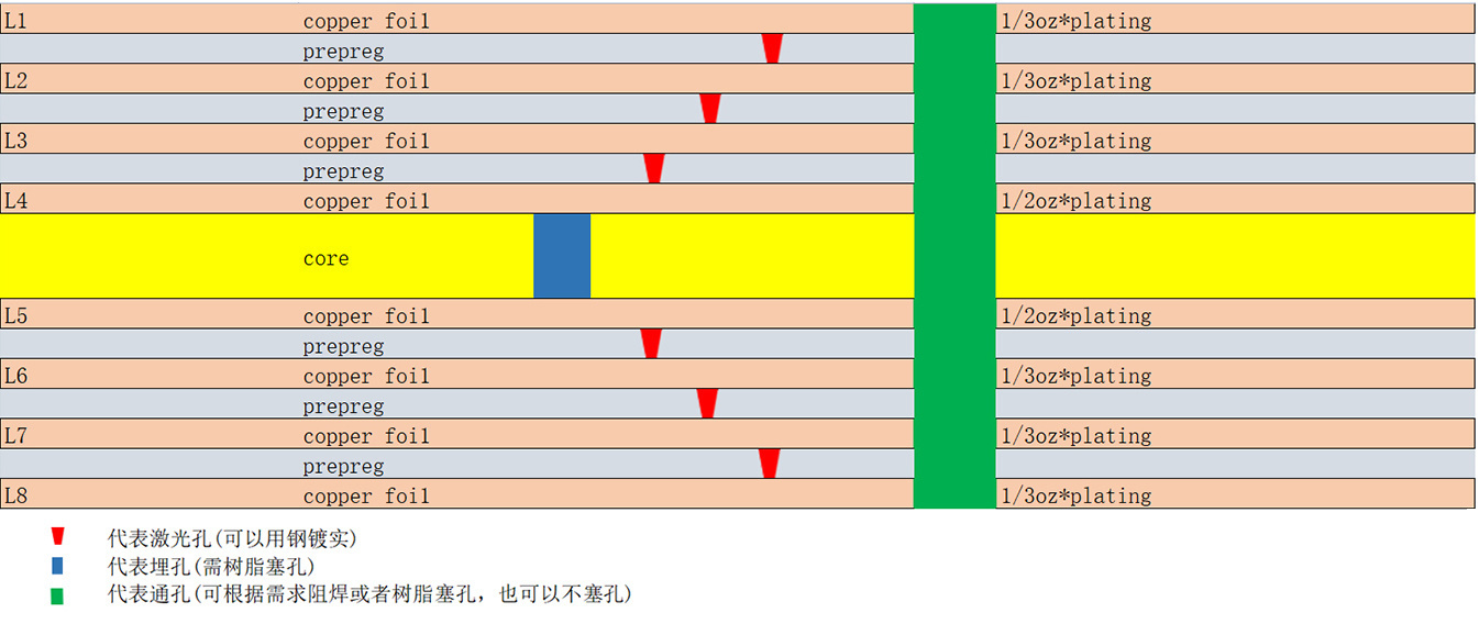
The image below shows a typical HDI board structure. To meet the requirements of HDI board manufacturing, we typically use 1/3 oz or 1/2 oz copper foil. Meanwhile, to ensure that the laser vias can penetrate the interlayer polypropylene (PP), we generally recommend designing the interlayer PP thickness for the laser vias to be < 0.1 mm. Therefore, if you have impedance control requirements and have designed laser vias, you need to consider the impact of thin PP on impedance. If you have any questions in this regard, please feel free to contact us.
|
|
|
|
|
Juyuan Union offers free simulation calculations of stack-up and impedance based on your requirements. Whether you need some advice on stack-up or want a complete stack-up impedance calculation, we are dedicated to serving you. We can collaborate with your engineering team during the PCB design phase, helping you achieve better results in impedance control by suggesting suitable PCB laminates and stack-ups.
Regarding stack-up impedance control, Bitelli can provide:
Free stack-up design
Free impedance calculation
Mixed laminate structures
RF (Radio Frequency), Microwave, and other high-frequency PCBs
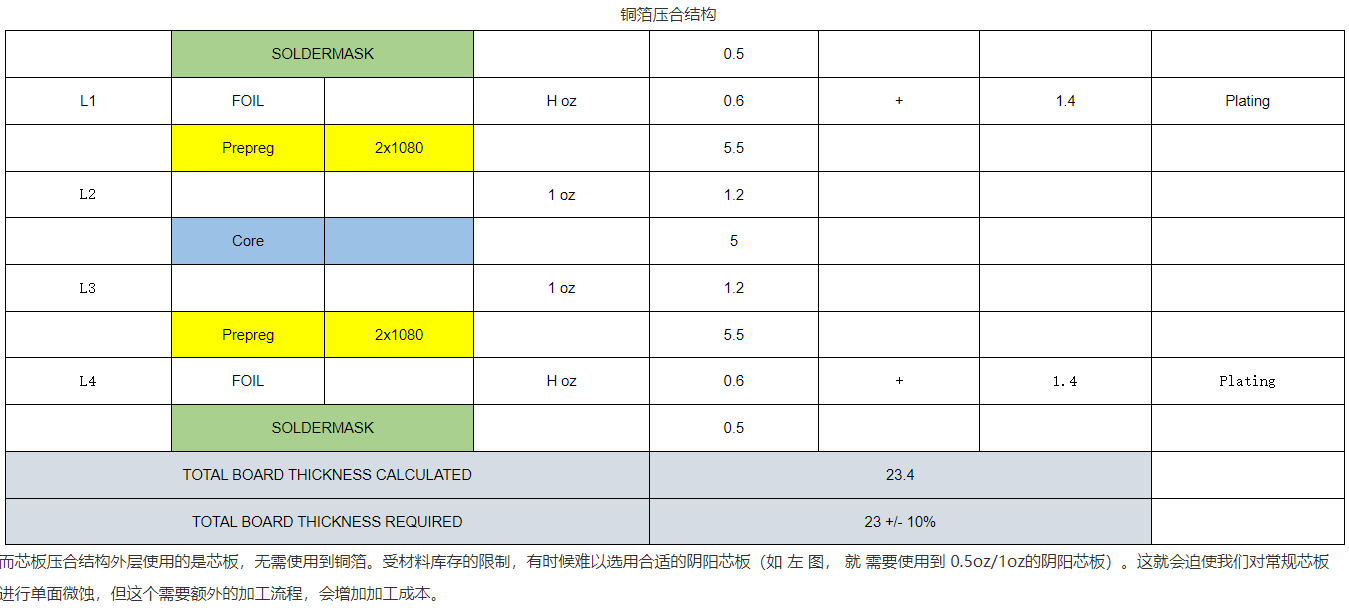
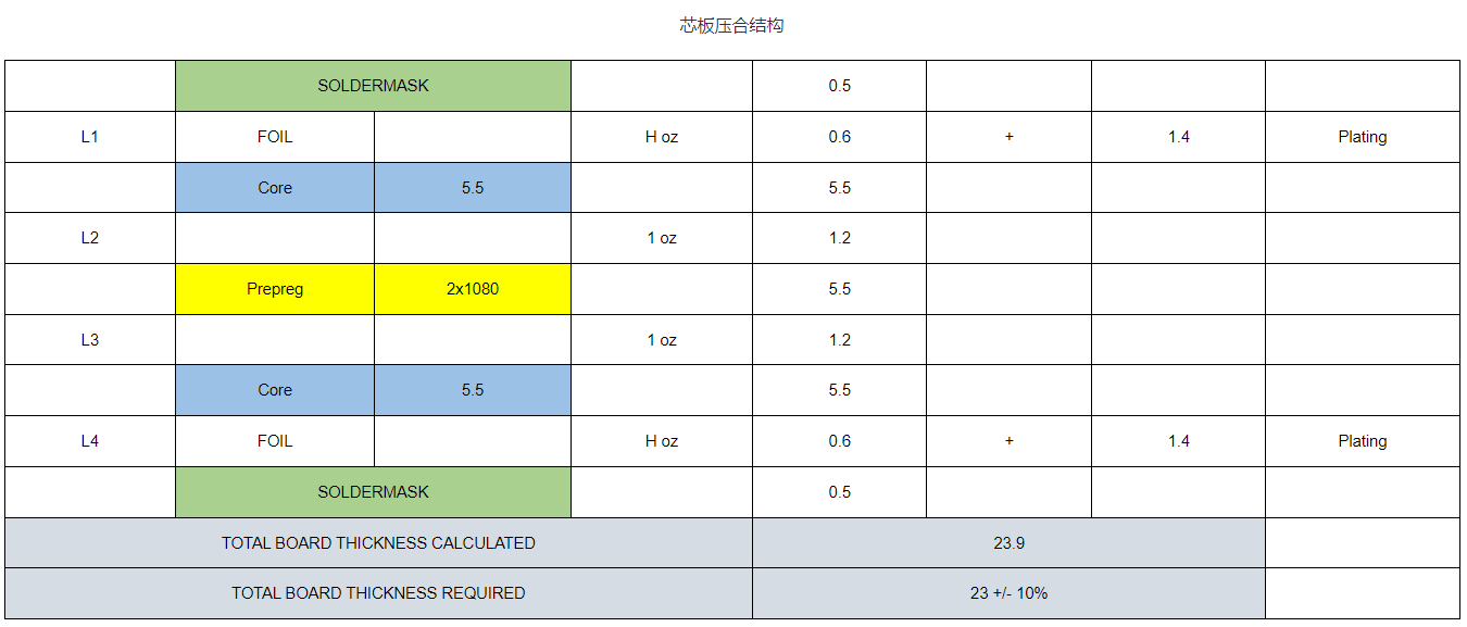
Choice between copper foil lamination and core board lamination structures
At Juyuan Union, we generally prefer copper foil lamination for optimal cost. We also offer the flexibility to use core board lamination. However, copper foil lamination boards are not only more economical than core board lamination boards, but also easier to manufacture. The diagram below illustrates the differences between copper foil laminated boards and core board laminated boards.
As shown in the diagram, the outermost layer of a copper foil laminated board is made of copper foil, requiring one less core board than a core board laminated board, resulting in lower costs. Furthermore, because copper foil is more readily available than core boards, copper foil laminated boards can avoid the use of certain male and female core boards, thus better meeting delivery timelines.
|
 |
 |
|
Regarding Impedance Calculation
Juyuan Union uses Polar SI8000 to calculate impedance. If the board has impedance requirements, we can provide an impedance test report and impedance test strips free of charge upon shipment. Typically, designers use the PP thickness provided in the material specification to calculate impedance. However, based on years of processing experience, we use the thickness of the PP after pressing to calculate impedance. Using the pressed thickness data optimizes our impedance calculation results, making them closer to the impedance on the finished board. This is why we encourage you to collaborate with our team during the design phase so we can help you optimize your impedance calculations.
We will add two impedance strips to the production panel, placing them diagonally, to check if the impedance within the board is acceptable. As mentioned above, we can provide an impedance test report and impedance test strips free of charge.
For impedances below 50 ohms, our standard impedance tolerance is +/- 5 ohms; for impedances above 50 ohms, our standard impedance value is +/- 10%. If required by the customer, we can achieve a tolerance of +/- 5%, but this will incur higher additional costs.
|
|
|
|
|
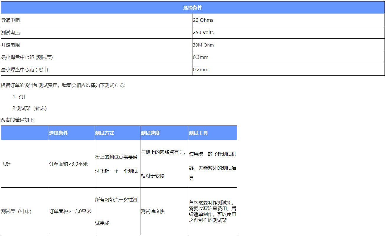
Juyuan Union conducts 100% electrical testing on its manufactured PCBs according to the IPC-9252 standard. There are typically two testing methods: one using flying probes, and the other using a test fixture.
To avoid discrepancies between the actual manufactured boards and the netlist relationships in the Gerber datasheet, we extract test points from the Gerber datasheet and perform testing according to the netlist relationships. We also request that you provide an IPC netlist file so we can compare it with the Gerber file. Since the netlist relationships in the IPC netlist file are defined before generating the Gerber file, it allows us to check if the generated Gerber file's netlist matches the requirements and avoid errors during Gerber file generation.
For the netlist file, we prefer that you provide it in IPC 356 format, as our software can recognize this format.
Testing Capabilities and Methods
Our testing parameters are as follows:
|
 |
|
Test Reports
We can provide the following reports free of charge upon request:
1. Cross-section report
2. X-ray inspection report
3. Cross-section report
4. Solderability test report
5. Impedance report (if the design includes impedance)
6. Withstand voltage test report
7. Peel strength report
8. COC (Conformity Certificate)
9. RoHS report
10. UL certification
|
|
|
|
 |
Number of layers: 2
Board thickness: 1.6mm
Surface treatment: Immersion gold
Solder resist color: Green
Aluminum substrate + 3oz copper
|
|
|
 |
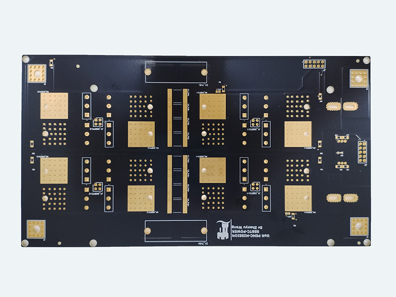
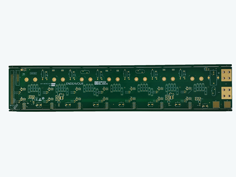
Number of layers: 16
Board thickness: 2.3mm
Surface treatment: Immersion gold
Solder mask color: Green
Blind vias, through-hole vias
|
|
|
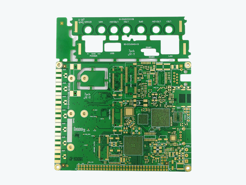 |
Number of layers: 6
Board thickness: 1.6mm
Surface treatment: Immersive gold
Multiple board types, complex shapes
2nd stage HDI board
|
|
|
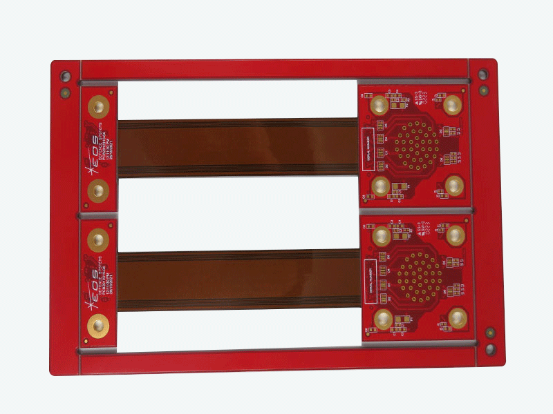 |
Number of layers: 8
Board thickness: 1.6mm
Solder resist color: Red
Rigid-flex PCB
Impedance control
|
|
|
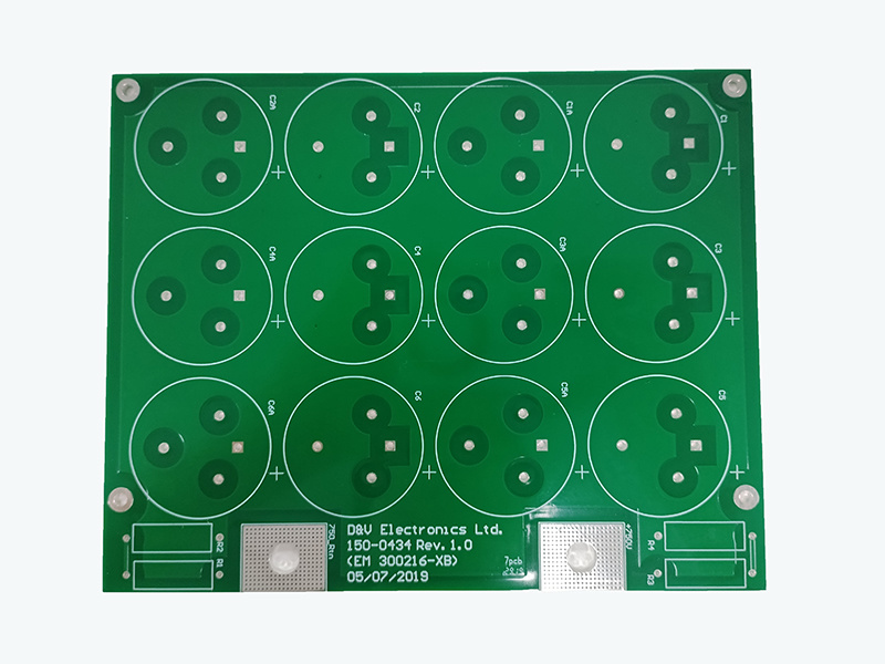 |
Number of layers: 6
Board thickness: 2.67mm
Surface treatment: Lead-free tin plating
Solder mask color: Green
Inner and outer copper thickness: 4oz
|
|
|
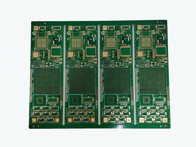 |
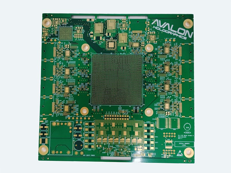
Number of layers: 10
Board thickness: 1.6mm
Surface treatment: Immersion gold
Any layer interconnect HDI
Impedance control, 3/3mil lines
|
|
|
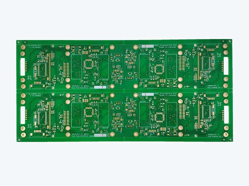 |
Number of layers: 2
Board thickness: 1.6mm
Surface treatment: Immersion gold
Solder mask color: Green
Some pads have carbon ink applied
|
|
|
 |
Number of layers: 6
Board thickness: 3.25mm
Surface treatment: Immersion gold
Solder mask color: Green
Extra-thick copper (10oz inner layer & 7oz outer layer)
|
|
|
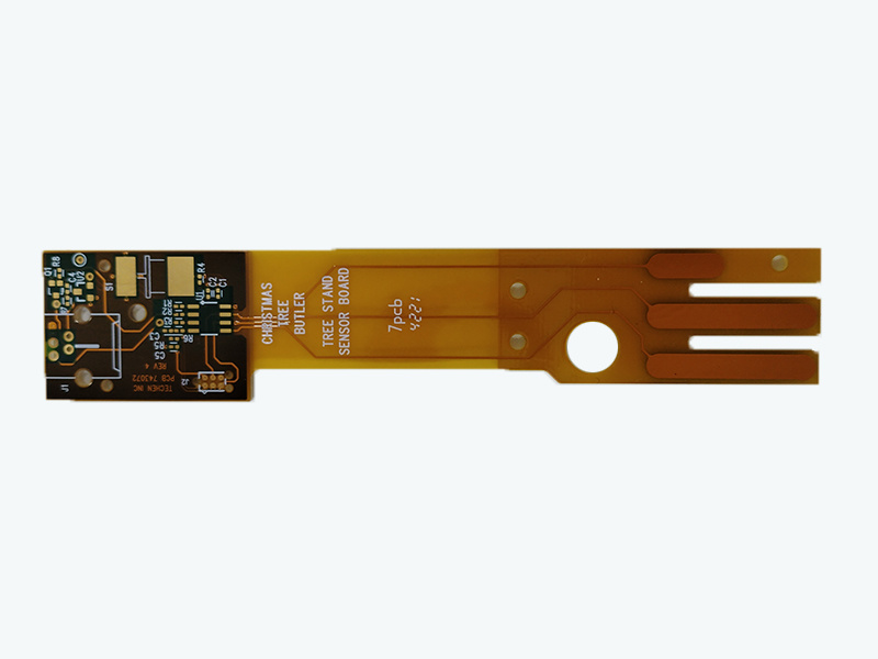 |
Number of layers: 2
Board thickness: 0.1mm
Surface treatment: Immersion gold
Cover film: Yellow
Local reinforcement applied
|
|
|
|
|
|
|
|
|
|